Plasmonic nanoparticles can concentrate electromagnetic energy on the nanometer scale, offering promising applications in diverse fields such as miniaturized photonic circuits or lab-on-chip. An essential prerequisite for these applications is efficient coupling between the nanoparticles and the excitation signal. Plasmonic nanoparticle chains are capable of guiding light on a sub-wavelength scale, and can be excited by being coupled to a dielectric waveguide. Here, a team from C2N proposes a new structural configuration that allows on-demand positioning of the chain relative to the waveguide. The existence of a critical coupling regime between a silicon waveguide and a plasmonic chain is demonstrated experimentally and numerically, enabled by precise control of their relative distance. In this regime, the plasmonic chain switches from its well-known transmission mode to a new resonant cavity state, depending on the strength of the coupling between the guide and the chain. In the region of critical coupling, virtually all the energy of the waveguide mode is trapped in the chain, resulting in a reduced group velocity and high spatial confinement with a narrow spectral response. This result paves the way for optimal addressing of nanostructures via integrated waveguides, resulting in highly efficient nanotweezers or optical nanoheaters. In addition, slowing down the group velocity enhances light-matter interactions and could be beneficial for catalytic amplification and sensors. Finally, coupling these structures with a phase-change material could enable the development of advanced nanotunable optical devices
Références
Critical coupling in plasmonic chain for efficient energy trapping.
Marius Crouzier1,3, Fei Mao1, Giovanni Magno2, Vy Yam1, Carlos Alonso-Ramos1, Jean-René Coudevylle1, Etienne Herth1, Christophe Dupuis1, Xavier Leroux1, Thomas Lopez3 & Béatrice Dagens1
Sci Rep 15, 22072 (2025)
DOI : https://doi.org/10.1038/s41598-025-05446-7
Affiliations
1Université Paris-Saclay, CNRS, Centre de Nanosciences et de Nanotechnologies, Palaiseau, 91120, France
2Department of Electrical and Information Engineering, Polytechnic University of Bari, Via Orabona, 4, Bari, 70125, Italy
3Centre technique de Vélizy, Stellantis, Vélizy-Villacoublay, 78140, France
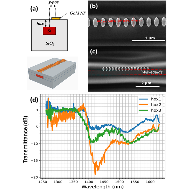
Figure : (a-b) Sketch of the structure investigated. The Si waveguide is encapsulated in a SiO2 cladding. The cladding height hox can be adjusted during the fabrication process. The resulting flat surface above the waveguides enables nanoparticle chains to be positioned with a lateral shift y-pos relative to the waveguides. (c-d) SEM images of the sample, with ypos = 410 nm. (d) Measured waveguide transmittance for 15 NP chains and different values of hox : hox1 = 35 ± 5 nm, hox3 = 75 ± 5 nm, and hox2 is between these two values. The lateral shift is constant for the three chains y-pos = 300 nm. The minimum transmittance, corresponding to the critical coupling regime, is reached at hox = hox2.
Contact : Béatrice Dagens
Key words : plasmons; integrated photonics; critical coupling; temporal coupled-mode theory; nanoparticle chain