For a long time optics evolution was based on the exploitation of the properties of so-called "natural" optical media, which are homogeneous and continuous on the wavelength scale. The advent of metamaterials dawned the era of new artificial media with exotic properties not encountered in the nature, leading to the demonstration of the invisibility cloak or the perfect lens based metamaterials with a negative index. However most of these demonstrations are confined to the field of microwaves.
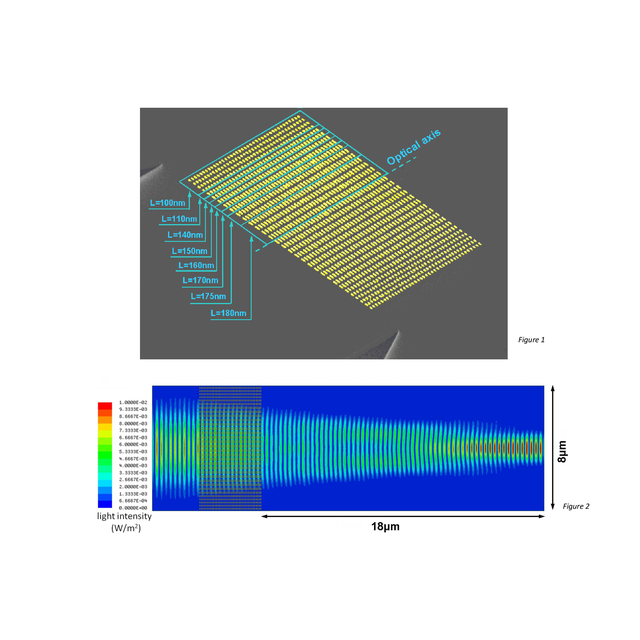
The two main obstacles preventing the use of metal metamaterials in the field of optics are: i) the technological difficulty of manufacturing multilayer structures; ii) the optical losses due to absorption of the metal. To circumvent these issues we consider a composite guiding structure made of a 2D plasmonic metasurface located on the top of high index silicon on insulator waveguide. The objective is to achieve an efficient control over the flow of the light in the waveguide using effective index variation induced by the metasurface resonance.
By following this approach our team performed the demonstration of the first plasmonic metasurface based graded index lens integrated on a Silicon waveguide for operation in the near infrared domain. This enabling technology is quite generic and can be adapted to different type of planar lightwave circuits platforms: Silicon, GaN/AlN, InGaAsP/InP, doped silica glass etc.
Reference:
Integrated 2D graded index plasmonic lens on a Silicon waveguide for operation in the near infrared domain,
Y. Fan, X. Le Roux, A. Korovin, A. Lupu & A. de Lustrac
ACS Nano 11, 4599–4605 (2017) / DOI : https://doi.org/10.1021/acsnano.7b00150
Figure: Y. Fan & al., ACS Nano (2017)