The C2N, in collaboration with the CEA and CEA/LETI in Grenoble, as well as the Center for Energy Research in Budapest (Hungary), has demonstrated superconductivity in thin layers of silicon-on-insulator (SOI) fabricated by nanosecond laser annealing under ultra-high vacuum. This process, compatible with large-scale microelectronics, was applied to 300mm SOI wafers with a 33 nm thick layer, heavily implanted with boron. A state-of-the-art critical temperature Tc=0.5Tc=0.5 K was achieved through the understanding and optimization of the electrical and structural properties of the annealed layers in relation to laser energy and the number of successive annealing steps. This work, published in APL Materials (2024), paves the way for the integration of superconducting silicon into microelectronics.
Superconducting monocrystalline Silicon On Insulator thin 33 nm epilayers are obtained by nanosecond laser annealing under ultra-high vacuum. The process is compatible with large scale microelectronics, and is performed on 300 mm wafers heavily preimplanted with boron (2.5 x 1016 cm-2, 3 keV). Superconductivity is discussed in relation to the structural, electrical and material properties, a step towards the integration of ultra-doped superconducting Si. In particular, we highlight the effect of the nanosecond laser annealing energy and the impact of multiple laser anneals. Increasing the energy leads to a linear increase of the layer thickness, and to the increase of the superconducting critical temperature Tc from zero (< 35 mK) to 0.5 K. This value is comparable to superconducting Si layers realised by Gas Immersion Laser Doping where dopants are incorporated without introducing the deep defects associated with implantation. Superconductivity only appears when the annealed depth exceeds the initial amorphous layer induced by the boron implantation. Multiple subsequent anneals result in a more homogeneous doping with reduced amount of structural defects and increased conductivity. The quantitative analysis of Tc concludes on a superconducting-non superconducting bilayer with an extremely low resistance interface. This highlights the possibility to couple efficiently superconducting Si to Si channels.
References
Nanosecond laser annealing: Impact on superconducting silicon on insulator monocrystalline epilayers
Y. Baron1, J. L. Lábár2, S. Lequien3, B. Pécz2, R. Daubriac4, S. Kerdilès4, P. Acosta Alba4, C. Marcenat5, D. Débarre1, F. Lefloch5, F. Chiodi1
APL Mater. 12, 121101 (2024)
https://doi.org/10.1063/5.0231177
Affiliations
1CNRS, University Paris-Saclay, Centre de Nanosciences et de Nanotechnologies, 91120 Palaiseau, France
2Thin Film Physics Laboratory, Institute of Technical Physics and Materials Science, Centre of Energy Research, Konkoly Thege M. u. 29-33, H-1121 Budapest, Hungary
3University Grenoble Alpes, CEA, IRIG-MEM, 38000 Grenoble, France
4University Grenoble Alpes, CEA, LETI, Minatec Campus, 38000 Grenoble, France
5University Grenoble Alpes, CEA, Grenoble INP, IRIG-PHELIQS, 38000 Grenoble, France
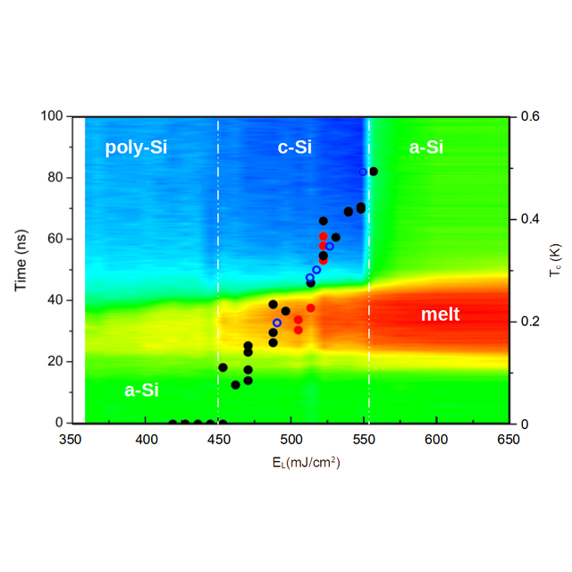
Figure :
Figure 1 : Combined plot of Time Resolved Reflectometry TRR and superconducting critical temperature Tc as a function of the laser energy density EL. The dotted line at EL = 450 mJ/cm2 indicates the cross-over from a polycrystalline boron doped layer to a crystalline epilayer. The dotted line at EL = 560mJ/cm2, where Rsq diverges, corresponds to the full melt of the initial silicon on insulator layer as the annealing touches the amorphous SiO2 BOX. The TRR color plot scale corresponds to the measured TRR amplitude from 0.75 RSi (dark blue) and 2.26 RSi (red), and is a signature of the layer structure : amorphous (green), polycrystalline (light blue), monocrystalline (dark blue), liquid (red). The laser pulse starts at t=10 ns.
Contact C2N : Francesca Chiodi