
PhD defense
(in french)
Centre de Nanosciences et de Nanotechnologies, Amphithéâtre,PhD defense
New concepts for the development of polaritonic emitters in the mid-IR and THz range
Centre de Nanosciences et de Nanotechnologies, Amphithéâtre,PhD defense
Jury members :
Aloyse Degiron, Chargé de recherche, MPQ Paris : Rapporteur & Examinateur
Karl Unterrainer, Professeur, TU Wien : Rapporteur & Examinateur
Aristide Lemaitre, Directeur de recherche (HDR), C2N Palaiseau: Examinateur
Eva Monroy, Docteure, NPSC Grenoble: Examinatrice
Raffaele Colombelli, Directeur de recherche (HDR), C2N Palaiseau: Directeur de thèse
Jean-Michel Manceau, Chargé de recherche, C2N Palaiseau: Coencadrant
Abstract :
The mid-infrared and terahetz bands of the electromagnetic spectrum have seen significant growth in applications in recent years, both in telecommunications and in the environmental and medical sciences.This interest is driving the demand for ever more compact and efficient sources and detectors. In this context, the development of coherent photon sources using the strong light-matter coupling regime is a promising avenue. Two axes of study of such sources will be explored in this thesis. First, a new approach to obtain mid-infrared photon emission through resonant optical pumping of intersubband polaritons was studied.
This type of spontaneous emission is based on the use of non-dispersive cavities, allowing in principle to increase the phonon-polariton scattering rate and thus to reach more easily the threshold intensity of the coherent emission. The demonstration of photon emission in this configuration opens up the possibility of exploring this emission in a stimulated scattering regime by populating the final state of the system with a probe beam.
In a second step, the focus will be on the THz domain. In order to overcome the thermal limitation imposed by the low energy of THz transitions, interdigitated parabolic quantum wells can be used to obtain resonant absorption up to 300K.To overcome the broadening introduced by multiple interfaces, alloy gradient wells were developed in collaboration with the University of Waterloo, Canada. This design resulted in very high quality THz transitions and an improvement in the operating temperature of the strong coupling regime by 170K. A particularity of intersubband polaritons is the possibility to obtain a high coupling constant through doping of the semiconductor.
Consequently, these polaritons have been a platform of choice for demonstrating the ultra-strong coupling regime, in which the fundamental level of the system is populated by a non-negligible population of virtual photons. Theoretical studies have predicted that a non-adiabatic modulation of the ground state of the system, i.e. on a time scale smaller than the lifetime of the polaritons, this pool of light can be accessed. It is then possible to see these virtual photons being emitted as real photons. To explore this effect, three-dimensional LC cavities have been functionalised to achieve ultra-fast switching of their resonant frequency.
Their development and characterisation by time-resolved THz spectroscopy will be presented.
By using low temperature epitaxial GaAs, sub-picosecond modulation times have been achieved.
Finally, the combination of these ultrafast switches with parabolic graded alloy quantum wells has allowed the achievement of a strong light-matter coupling regime between them.
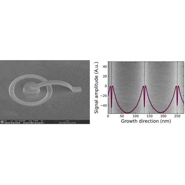
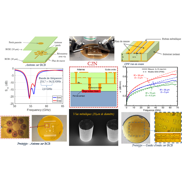
Figure 1: SEM image of a 3D LC resonator with parabolic quantum well active region in the patch. Figure 2: STEM image of a continuously graded parabolic quantum well. Overlay alloy profile extracted from the STEM signal amplitude.
Hybrid integration for on-chip optical emission and amplification in the near infrared
Centre de Nanosciences et de Nanotechnologies, Amphithéâtre, PalaiseauPhD defense
Jury members :
Yannick DUMEIGE, Professeur des universités, FOTON (UMR 6082), Université de Rennes 1, Rapporteur & Examinateur
Jean-Pierre VILCOT, Directeur de Recherche, IEMN (UMR 8520), Université de Lille, Rapporteur & Examinateur
Lionel BASTARD, Maître de conférences, IMEP-LaHC (UMR 5130), INP - Phelma, Examinateur
Philippe DELAYE, Directeur de Recherche, LCF (UMR 8501), IOGS, Examinateur
Éric CASSAN, Professeur des universités, C2N (UMR 9001), Université Paris-Saclay, Directeur de thèse
Abstract :
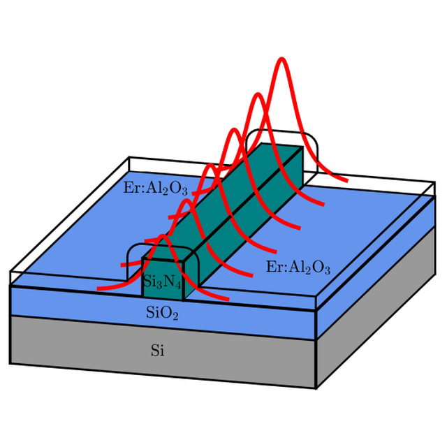
One of the main challenges in the field of silicon photonics is to develop integrated optical sources and optical on-chip amplifiers. This thesis provides a contribution to the investigation of Erbium-based on-chip amplifiers and lasers. One main axis of the work carried out is to seek miniaturization of the active waveguides (<1mm, or even <<1 mm) and systematically consider a silicon integration perspective by favoring 1480 nm pump wavelength scheme.
Active SiN waveguides coated with Erbium-doped Al2O3 layers at more than 1021 cm-3 and deposited by the ALD technique at Aalto university are the basis for the experimental demonstrations in this work. Modal gains of 10-20 dB/cm are demonstrated in these waveguides. Capitalizing on these results, theoretical and simulation work is further carried out in the purpose of investigating aggressive designs in terms of active structure lengths. Different types of single and double resonant cavities and resonators are studied and designed for the realization of integrated sources using the measured properties of experimentally studied active waveguides. As a whole, the carried out works contribute to the realization of compact light sources in silicon photonics exploiting recent advances in the growth of rare-earth doped active layers and the design of multiply resonant resonators.
Link : https://teams.microsoft.com/l/meetup-join/19%3ameeting_NTNjMjVjYjMtZWRiMC00NjI4LThiMjYtNjYwMzgzYzExZTJm%40thread.v2/0?context=%7b%22Tid%22%3a%2268cdfebb-157b-4846-ba2f-d196a9124ac0%22%2c%22Oid%22%3a%2229dc529d-e78a-4197-ba7b-d7b7145626b5%22%7d

Switchable photovoltaic properties in ferroelectric PZT thin films
Centre de Nanosciences et de Nanotechnologies, Amphithéâtre,PhD defense
Jury members :
Houssny BOUYANFIF, Rapporteur, Maître de conférences-HDR, Université de Picardie (LPMC)
Bohdan KUNDYS, Rapporteur, Chargé de recherche, HDR, Université de Strasbourg, CNRS
Laurent DANIEL, Examinateur, Professeur des universités, Université Paris-Saclay
Maryline GUILLOUX-VIRY, Examinatrice, Professeur des universités, Université de Rennes 1
Hélène MAGNAN, Examinatrice, Ingénieure de recherche CEA
Philippe LECOEUR, Directeur de thèse, Professeur, Université Paris-Saclay (C2N)
Sylvia MATZEN, Encadrante, Maître de conférences, Université Paris-Saclay (C2N)
Thomas MAROUTIAN, Invite, Chargé de recherche, Université Paris-Saclay-CNRS
Abstract :
Ferroelectric (FE) thin films are being explored for their possible use in photovoltaic (PV) applications. This is due to their high open-circuit voltage and switchable photovoltaic effect, which make them attractive for PV applications. Theoretically, 100% switching of the photocurrent can be achieved by varying the direction of the ferroelectric polarization through the ferroelectric layer. This is particularly intriguing for applications such as photo-ferroelectric memory. The presence of switchability in integrated ferroelectric films between electrodes, however, is not always achieved due to extrinsic parameters such as the nature of the electrode-ferroelectric interface (Schottky contact) or the presence of non-mobile charged defects in the ferroelectric film. In addition, the movement of charged defects, such as oxygen vacancies, under the influence of applied electric fields can have an effect on switchable photocurrent as well. It is not an easy process to disentangle all these contributions (polarization, interfaces, defects) to the photovoltaic properties of ferroelectric devices, and little is known about the quantitative link between photocurrent and ferroelectric polarization.
In this work, a thorough investigation of the switchability of the PV properties of epitaxial lead zirconate titanate Pb(Zr,Ti)O3 (PZT) thin films has been carried out in order to study quantitatively the role of ferroelectric polarization. 100 nm thick PZT films were grown using pulsed laser deposition (PLD) and integrated into a capacitor geometry between bottom and top electrodes. The photoinduced current in the PZT devices was investigated under UV illumination (above the PZT band gap) and in different polarization states by poling the devices under increasing electric fields in order to achieve distinct electrical states while simultaneously monitoring their polarization value.
A comparison study of different interfaces was also carried out, including Pt and ITO as top electrodes, SrRuO3 (SRO) and LaSrMnO3 as bottom electrodes, as well as the insertion of SrTiO3 dielectric layer at the PZT/electrode interface. This work has provided a quantitative determination of the switchable vs unswitchable parts of photocurrent. More precisely, the study of the dependence of the photocurrent as function of electrically controlled remanent polarization has shown that (1) the photocurrent depends linearly on the switchable part of the ferroelectric polarization and that (2) the analysis of this dependence allows extracting quantitatively the pinned polarization value in the FE layer. Such pinned polarization strongly affects the switchability of the PV properties in FEs and is otherwise rather difficult to probe by classical FE characterizations. In addition, the comparison study of different interfaces also revealed the contribution from the electrode-ferroelectric interface on the PV properties, which can induce really different switchability and amplitude of photocurrents.
In conclusion, these results are thus particularly relevant for the optimization of FE thin films to achieve switchable PV properties which could have far-reaching implications for future photo-ferroelectric memory applications. In addition, the developed method of investigation of photocurrents switchability provides important insights on the ferroelectric behavior in all types of ferroelectric layers, in which pinned polarization could be significant but difficult to investigate otherwise.
Link: soon
Nanostructured III-nitride light emitting diodes
Centre de Nanosciences et de Nanotechnologies, Amphithéâtre, PalaiseauPhD defense
Jury members :
Jean-Christophe HARMAND, Directeur de Recherche, CNRS-C2N, France, Président
Enrique CALLEJA, Professeur, ISOM-UPM, Espagne, Rapporteur
Rachel GRANGE, Professeure, ETH, Suisse, Rapportrice
Benjamin DAMILANO, Chargé de recherche, CNRS-CHREA, France, Examinateur
Anna FONTCUBERTA i MORRAL, Professeure, EPFL, Suisse, Examinatrice
Maria TCHERNYCHEVA, Directrice de Recherche, CNRS-C2N, France, Directrice de thèse
Abstract :
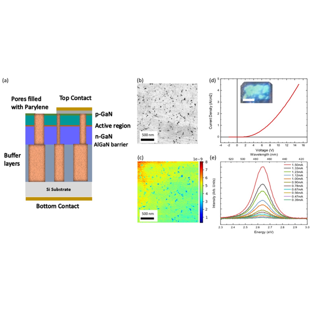
Flexible light emitting diodes (LEDs) are today a topic of intense research driven by applications such as bendable displays, conformable light sources, bio-medical devices, etc. The conventional inorganic semiconductor devices are mechanically rigid; the fabrication of flexible devices from thin film structures is quite challenging and requires micro-structuring and lift-off of the active layer. Instead of two-dimensional films, in this thesis two types of III-nitride nanostructures are studied: (i) a bottom-up strategy using core shell nanowires, and (ii) a top-down strategy using a porous structure.
Polymer-embedded nanowire membranes combine the high efficiency and the long lifetime of inorganic semiconductor materials with the high flexibility and transparency of polymers. I used MOCVD cores shell NWs for the fabrication of flexible blue and green NW LEDs, I also combined them with nanophosphors of different emission colors to produce a second generation of white LEDs with an improved color quality. For the fabrication of red flexible NW LEDs, I tested different strategies, namely an all-InGaN route based on In rich InGaN/GaN MQW NWs with a down-conversion of the blue light by a red phosphor and a red emission from GaAsP NWs.
Selective area sublimation was demonstrated to be a promising approach to improve the luminous efficacy of defective GaN layers on Si. In my work, I analyzed the impact of porosification on InGaN/GaN single quantum wells and on p-i-n light emitting diode structures. The optical analyses were performed by cathodoluminescence demonstrating that the high temperature sublimation process does not degrade the QW emission while electron beam induced current microscopy showed that the p-i-n junction profile is also preserved after sublimation. I also describe the optimization of the technology for porous LED fabrication following several strategies. As a result, I demonstrated the first porous InGaN/GaN blue LED using parylene pore filling for electrical insulation.
Link: soon
(in french)
Centre de Nanosciences et de Nanotechnologies, Amphithéâtre, PalaiseauPhD defense
Spin and valleys in layered materials
Centre de Nanosciences et de Nanotechnologies, Amphithéâtre, PalaiseauPhD defense
Jury members :
Franck Balestro, Rapporteur, Pr, Université Grenoble Alpes, Institut Néel, CNRS, Grenoble
Guillaume Schull, Rapporteur, Directeur de Recherche, Département Surfaces et Interfaces, IPCMS, CNRS, Strasbourg
Sophie Guéron, Présidente,Directrice de Recherche, LPS, CNRS, Orsay
Hervé Aubin, Directeur de thèse, Directeur de Recherche, C2N, CNRS, Palaiseau
Abstract :
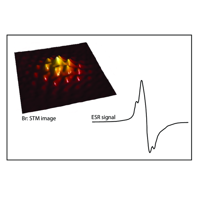
Quantum spin states constitute a resource for the development of quantum technologies. They have been considered for the realization of quantum computers, quantum simulators and quantum sensors. These long-term goals demand for the identification of appropriate hosts for quantum spin states with long coherence time and compatible with microfabrication technologies. Because of their two-dimensional character that enables an easier localization of the dopants in the material, monoatomic layer of Van-der-Waals materials is of intense interest. My Ph.D. describes experimental works that address two issues in this field. First, the identification of point-defects with interesting spin properties in Van-der-Waals materials; second, the Electrical Detection of Magnetic Resonance (EDMR) in those Van-der-Waals materials.
My work addresses two layered materials possessing spin and valley degrees of freedom: the Br-doped 2H-MoTe2 semiconductor belonging to the transition metal dichalcogenide (TMD) family and graphene. In 2H-MoTe2, we found that the electronic levels of the Br-dopants electronic levels are hybridized to the valleys in the conduction band. This produces spin-valley states where the spin and valley quantum numbers are locked. Moreover, by spin resonance methods, we find that the Br dopant carries an unpaired spin with coherence lifetime reaching 50 ns at the lowest temperature of 4.2 K. This is of practical interest as such states can be manipulated conveniently by electric fields. In graphene, encapsulated in hBN. we show that the spin resonance can be detected by transport measurements and propose a simple model relating the spin-resonant signal to the time average of the perpendicular magnetization component <Mz>.
Link: https://zoom.us/j/91310303583?pwd=T3JweDN1UDRWWFlPNVh6dFBla1BEdz09
ID de réunion : 913 1030 3583
Code secret : pHaPA4
(in french)
Centre de Nanosciences et de Nanotechnologies, Amphithéâtre, PalaiseauPhD defense
(in french)
Unité Mixte de Physique CNRS-Thales, Amphithéâtre, PalaiseauPhD defense