
PhD defense
Graded photonics crystals on SOI platform for near-infrared applications
Centre de Nanosciences et de Nanotechnologies, Amphithéâtre, PalaiseauPhD defense
Jury members :
Ségolène Callard, Professeure des universités, École Centrale de Lyon, Rapporteur
Emmanuel CENTENO, Professeur des universités, Université Clermont-Auvergne, Rapporteur
Éric LHEURETTE, Professeur des universités, Université de Lille, Examinateur
Olivier GAUTHIER-LAFAYE, Professeur des universités, Université Toulouse 3, Examinateur
Éric AKMANSOY, Maître de conférences(HDR), Université Paris-Saclay, Directeur de thèse
Anatole LUPU, Directeur de recherche, Université Paris-Saclay, Co-encadrant de thèse
Abstract :
Graded Photonic Crystals (GPC) allow to efficiently control the flow of light thanks to the shape of their photonic bands. But GPC in near infra-red was limited by a lack of easy-to-implement fabrication techniques. Nanotechnology enables us to efficiently fabricate photonic crystals, which we have implemented in this work. The main purpose of this thesis is to explore graded photonic crystals and related gradient index optics in the near-infrared domain for applications on Silicon On Insulator (SOI) platforms. According to the theory of subwavelength electromagnetism, the size of the device should be of the same order of magnitude as the operating wavelength. Thus, a big challenge in the NIR field is the fabrication and characterization of the corresponding devices. A significant part of this work is focused on the fabrication and characterization process of gradient photonic crystals in the NIR field. We have focused on nano-fabrication technology as well as SNOM characterization. SOI was chosen as the processing platform for this work, considering the good compatibility of the silicon-based platform with photonic devices and its ability to integrate well with nanofabrication techniques. In addition, another emphasized aspect of this work is to explore the effect of the variation of the photonic crystal parameters on its effective refractive index. Thus, the case of normalized frequencies in different photonic crystal energy bands has also been studied. We attempt to manipulate the effective refractive index (even negative refractive index) of photonic crystals by changing their parameters. Experimental demonstration of negative refractive index gradient photonic crystal lens and related gradient photonic crystal devices is highlighted.
(in french)
Centre de Nanosciences et de Nanotechnologies, Amphithéâtre,PhD defense
(in french)
Centre de Nanosciences et de Nanotechnologies, Amphithéâtre, PalaiseauPhD defense
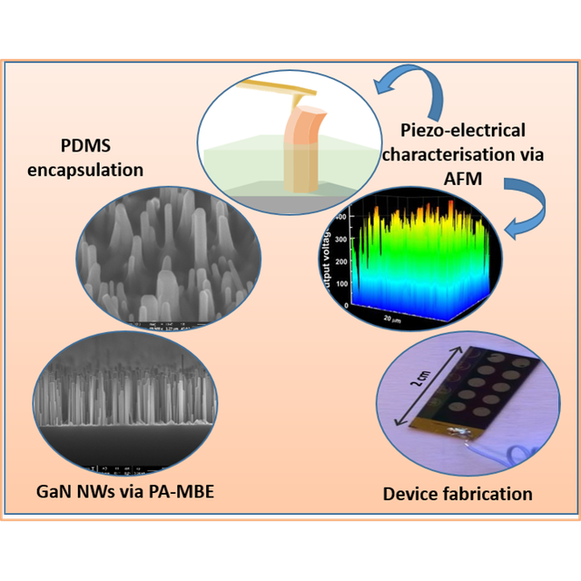
Novel solutions for piezogeneration enhancement in GaN nanowires
Centre de Nanosciences et de Nanotechnologies, Amphithéâtre, PalaiseauPhD defense
Jury members :
Gustavo Ardila, HDR, IMEP-LaHC, rapporteur
Brice Gautier, Professeur des Universités, INSA Lyon, rapporteur
Guylaine Poulin-Vittrant, DR2-CNRS, Greman, examinateur
Vincent Sallet, Chargé de Recherche CNRS, Gemac, examinateur
Christophe Durand, Maître de Conférences, CEA-Grenoble, examinateur
Noelle Gogneau, DR, C2N, directrice de thèse
Abstract :
In the last decade, GaN nanowires (NWs) have emerged as promising candidates in the field of small-scale energy harvesting. Their superior mechanical and piezoelectric properties confers to them the ability to effectively convert the ambient vibrational and mechanical energies into electrical energy, and thus develop a new generation of ultracompact, high-efficient and self-sustainable piezoelectric generators to assist or power microelectronic devices. Despite the demonstration of first promising NW-based piezo-generators, it is today indispensable to further increase the piezo-conversion capacity of these new harvesters. The exploration of novel solutions to enhance their performances is the research axis of this thesis. Here, plasma-assisted molecular beam epitaxy (PA-MBE) is employed to grow intrinsically p-doped GaN NWs with high crystalline quality. Thanks to a nano-characterization tool based on atomic force microscope equipped with the Resiscope electric module specifically adapted for piezoelectric conversion measurements, the piezoelectric response of NWs is investigated as a function of the explored solutions. The piezo-generation efficiency of the NWs is strongly affected by the external circuit. For the first time in the nanoscale regime. We experimentally demonstrate its influence on the piezo-generation efficiency of the NWs. The limitations of the formerly established protocol to judge the piezo-generation capacity of 1D-nanostructures are addressed and solutions are proposed. The piezo-generation efficiency of the NWs is also deeply affected by the surface charges, which are strongly pronounced in sub-100 nm wide GaN NWs. We demonstrate that these surface charges can be advantageous for piezoelectric applications as they offer the possibility to tune the free charge carrier concentration as a function of NW diameter. Thus, we establish experimentally that in the presence of surface charges, the electromechanical coupling efficiency of GaN NWs increases up to 43.4 % for diameters in the range of 45-60 nm. The piezoelectric measurements on GaN and GaN/Al2O3 core-shell NWs are also performed. The reduction of surface charge density by the Al2O3 shell results in a degradation of the piezoelectric response of the NWs. These results confirm the importance of the surface charges for improving the piezo-response of GaN NWs. Finally, by taking advantage of these solutions, output voltages reaching up to 520 mV per NW have been measured, stating a new-state-of-the-art, in the commonly used protocol, for 1D piezoelectric nanostructures.
(in french)
Centre de Nanosciences et de Nanotechnologies, Amphithéâtre, PalaiseauPhD defense
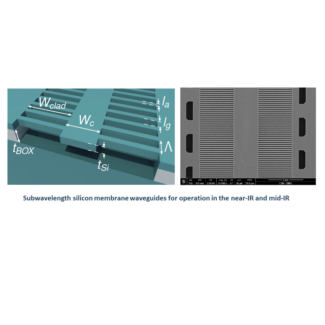
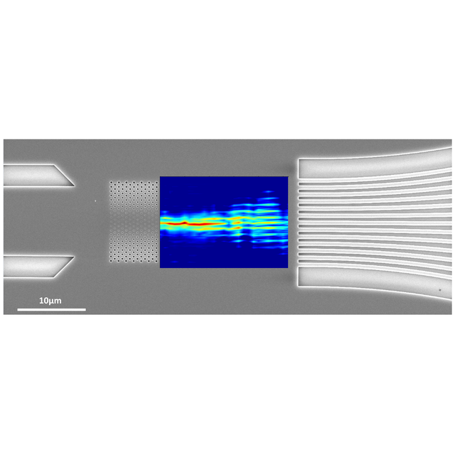
Subwavelength silicon photonic nanostructures for applications in the near-IR and mid-IR
Centre de Nanosciences et de Nanotechnologies, Amphithéâtre,PhD defense
Jury members :
Philippe DELAYE. Directeur de recherche, Institut d’Optique. (Universite Paris-Saclay) Président
Gonzalo WANGÜEMERT-PÉREZ. Professor, Málaga University Rapporteur & Examinateur
Emilien PEYTAVIT. Chargé de recherche, Laboratoire IEMN Rapporteur & Examinateur
Loïc BODIOU. Maitre de conferences, Universite de Rennes 1 Examinateur
Joan RAMIREZ Cadre scientifique, Nokia Bell Labs/ III-V lab Examinateur
Carlos ALONSO RAMOS Chargé de recherche, C2N-Université Paris-Saclay Directeur de thèse
Abstract :
Silicon photonics holds the promise for large-scale and low-cost production of highperformance optoelectronic circuits. Driven by the impressive technology development in the recent years, silicon photonics is expanding its frontiers towards new applications beyond datacom, including among others, sensing, radio-over-fiber and quantum. Aiming to meet the requirements of these new applications, the Si photonics community is exploring alternative wavelength ranges and physical phenomena, with a particular interest in the midinfrared (2-20 μm wavelength), and Kerr
nonlinearities. Silicon photonics holds the promise for large-scale and low-cost production of high-performance optoelectronic circuits. Driven by the impressive technology development in the recent years, silicon photonics is expanding its frontiers towards new applications beyond datacom, including among others, sensing, radio-over-fiber and quantum. Aiming to meet the requirements of these new applications, the Si photonics community is exploring alternative wavelength ranges and physical phenomena, with a particular interest in the mid-infrared (2-20 μm wavelength), and Kerr nonlinearities.
Understand and overcome the limitations of silicon/amorphous silicon (a-Si:H) nanowire solar cells
Centre de Nanosciences et de Nanotechnologies, Amphithéâtre, PalaiseauPhD defense
Jury members :
Anna Fontcuberta-i-Morral, Rapportrice & Examinatrice, Professeure, Ecole Polytechnique Fédérale de Lausanne (EPFL)
Erwann Fourmond, Rapporteur & Examinateur, Maître de conférences, INSA Lyon
José Alvarez, Examinateur,Chargé de recherche, Université Paris-Saclay, GEEPS
Jean-François Guillemoles, Examinateur, Directeur de recherche, Insitut Polytechnique de Paris, laboratoire IPVF
Maria Tchernycheva, Directrice de thèse, Directrice de recherche, Université Paris-Saclay, C2N
Martin Foldyna, Invité, Chargé de recherche, Insitut Polytechnique de Paris, LPICM
Abstract :
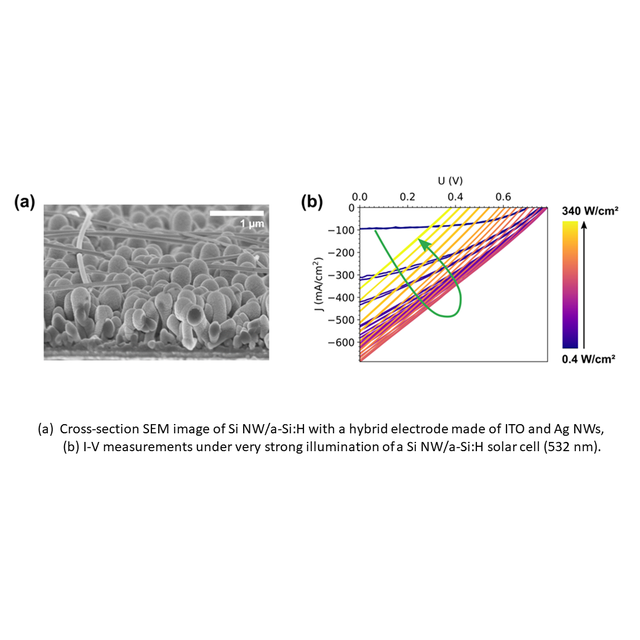
Among different materials for photovoltaic conversion, hydrogenated amorphous silicon (a-Si:H) displays excellent optical properties and can be used as a thin-film, requiring less material. However, the low mobilities of its charge carriers limit the efficiency in planar solar cells. Core-shell structures can solve this issue. This PhD work focuses on solar cells made of silicon/amorphous silicon (a-Si:H) core-shell nanowires (NWs). For these nanostructures the optimization of the top contact, which has to be both transparent and conductive is a major challenge. We developed a hybrid electrode, made of ITO and silver nanowires, to efficiently collect the charge carriers from every nanowire and over the whole cell (Fig. (a)). Changing the illumination level, we optimized the electrode transparency and conductivity directly on the device. The hybrid electrode increased the power conversion efficiency from 4.3 % to 6.6 % compared to the reference ITO electrode. In addition, we studied the change in performance of Si NW/a-Si:H solar cell under strong illumination (Fig. (b)). Amorphous silicon is generally believed to be suited only for low illumination levels, but there are no detailed studies on this topic, especially in a core-shell NW solar cell architecture. The comparison of I-V measurements of a Si NW/a-Si:H with a planar a-Si:H and a crystalline silicon solar cells evidenced different phenomena, both reversible and irreversible. In particular, it showed that the first limiting factors are not directly related to a-Si:H, but to the top-contact and the substrate.
Link: https://cnrs.zoom.us/j/96292459096?pwd=Q0JxcGx1MW9BTk9Hcm1KQUkrbE52dz09
Passcode: HCqyW4
Find a link in the the attached file below
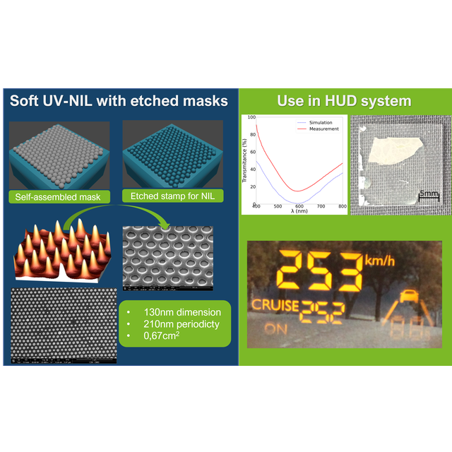
Development of resonant nanostructures large area device for augmented reality
Centre de Nanosciences et de Nanotechnologies, Amphithéâtre,PhD defense
Jury members :
Cécile GOURGON, Directrice de Recherche, Université Grenoble Alpes, Rapporteur
Aloyse DEGIRON, Chargé de Recherche, Université de Paris, Rapporteur
Anne-Marie HAGHIRI-GOSNET, Directrice de recherche, Université Paris-Saclay, Examinatrice
Daniel TUROVER, Ingénieur, SILSEF, Examinateur
Serge RAVAINE, Professeur, Université de Bordeaux, Examinateur
Rose-Marie SAUVAGE, Responsable Innovation, Agence Innovation Défense, Invitée
Béatrice DAGENS, Directeur de recherche, Université Paris-Saclay, Directrice de thèse
Frédéric HAMOUDA, Ingénieur de recherche, Université Paris-Saclay, Encadrant technologique
Abstract :
Recently, visualisation systems, and in particular augmented reality, have seen increased use in applications such as automotive head-up displays or head-mounted displays such as Google Glass. Due to the cost constraints of industrial applications, technological solutions are needed to improve the efficiency of these devices. In particular, these systems include a large surface blade that must be both transparent in the visible range and reflective at certain wavelengths. It can also perform the function of focusing or defocusing.
In this context, wavelength-selective reflective metasurfaces are considered good candidates. This type of device has attracted a lot of attention in recent years due to the unique properties that can be obtained but nevertheless, significant improvements are still needed to make it a viable option.
Link: https://us02web.zoom.us/j/86341050123?pwd=WmVDOHdHYXpoazRwNTNqSmFXVHBvUT09
Find a link in the the attached file below
Non-linear physics associated to chiral symmetry in driven dissipative polariton lattices
IOGS, Auditorium, PalaiseauPhD defense
Jury members :
Mme Jacqueline BLOCH Université Paris-Saclay GS Physique, Directrice de thèse
M. Christian SCHNEIDER Carl von Ossietzky Universität Oldenburg Institut für Physik, Rapporteur
Mme Anna MINGUZZI Laboratoire de Physique et Modélisation des Milieux Condensés, Rapporteure
M. Iacopo CARUSOTTO INO-CNR BEC Center and Dipartimento di Fisica, Università di Trento, Examinateur
Mme
Emmanuelle DELEPORTE Ecole Normale Supérieure Paris-Saclay Examinatrice
M. Sylvain NASCIMBENE Laboratoire Kastler Brossel, Collège de France Examinateur
M. Sylvain RAVETS Invité
Abstract :
Microcavity polaritons originate from the strong coupling between cavity photons and electronic excitations of a semiconductor microcavity. These quasi-particles inherit properties from both constituents: the electronic component is responsible for giant Kerr non-linearities while the photonic part makes the system inherently dissipative and allows confining polaritons in micro-structures obtained via etching of the cavity. This thesis presents the study of the non-linear properties of micro-cavity arrays with chiral symmetry.
The first part of the work is dedicated to one-dimensional topological lattices emulating the Su-Schrieffer-Heeger model. In the non-linear regime, driving the system coherently using a laser leads to the formation of gap solitons at the edges and in the bulk of the structure. We evidenced that such solitons present symmetry properties making them robust against certain types of defects. In addition, we unveiled that a careful engineering of the drive allows observing novel non-linear solutions which are specific to open systems. We analyzed the systems excitations spectrum in presence of such stationnary state and demonstrate the possibility to realize a topological phase transition induce by the interactions.
In the second part, we explored the properties of the interaction between two gap solitons and showed that the interaction sign is strongly linked to the underlying structure of the lattice. This work showed the presence of a spontaneous symmetry breaking. The study of the systems non-linear response in the vicinity of such phase allows us to discover a novel effect of bistability allowing to induce chirality in the system depending on the drive protocol. We called this effect “helical bistability”. The helical bistability is a very general effect that can be observed in a simple set of two coupled Kerr resonators and is linked to the physics of a particle with spin one half. These results are supported both by numerical simulations and experiments. This thesis illustrates how symmetries and non-linearities enriches the physics of photonic systems in a driven-dissipative context.
If you plan to attend the defense in person, please fill in the following document: https://docs.google.com/spreadsheets/d/1p3-8EWfpD3NS8eQNAhk4CfH4_3KzzVQ0819CWU8K6Ko/edit?usp=sharing
Link: https://zoom.us/j/94169025971?pwd=VDJkUkxZZXBMUXl2aCtYN054blErQT09
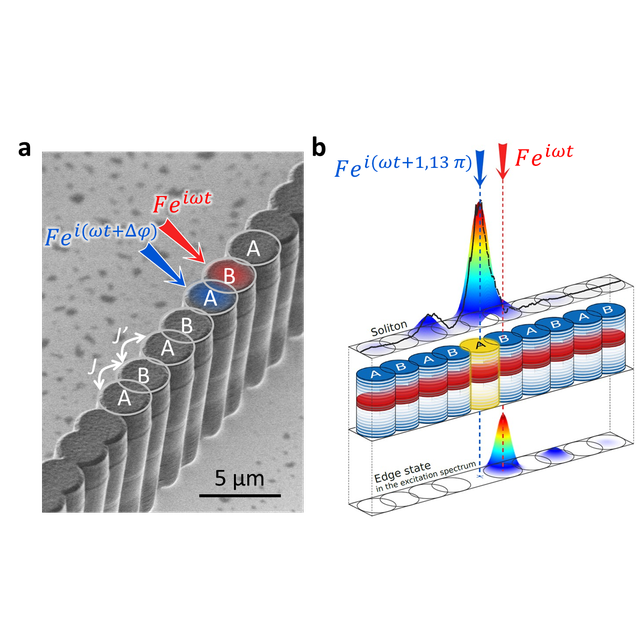
Caption: (a) Scanning electron microscopy image showing a chain of semiconductor cavities. The distance between the cavities is modulated, which gives rise to two different values of the coupling J and J’ between adjacent cavities (represented schematically by double white arrows). This modulation of the coupling provides the lattice with topological properties. Two cavities of the lattice are excited by two lasers of amplitude F, angular frequency w and presenting a phase difference Dj. b) For Dj =1.13p, we have demonstrated a new family of solitons, which measured intensity profile is shown at the top of the figure. The intensity is very strong on one single site, thus leading to the spectral detuning of this site with respect to the rest of the chain. The chain is thus effectively broken, and an edge state appears in the excitation spectrum, as shown at the bottom of the figure.
Collage III-V//Si par couches transparentes conductrices pour cellules solaires tandem
Centre de Nanosciences et de Nanotechnologies, Amphithéâtre,PhD defense
Jury members :
M. Stéphane COLLIN, Université Paris-Saclay GS Sciences de l’ingénierie et des systèmes,Directeur de thèse
Mme Anne KAMINSKI-CACHOPO,Grenoble INP-Phelma ,Rapporteure
M. Yvan CUMINAL, Université de Montpellier, Rapporteur
Mme Anne TALNEAU, Université Paris-Saclay - C2N - CNRS, Examinatrice
M. Romain CARIOU, CEA Liten, Examinateur
M. Andrea CATTONI, Université Paris-Saclay - C2N - CNRS, Co-encadrant de thèse
M. Philippe BARANEK, EDF R&D – Departement SYSTEME, Invité
M. Oliver HöHN, Fraunhofer Institute for Solar Energy Systems ISE, Invité
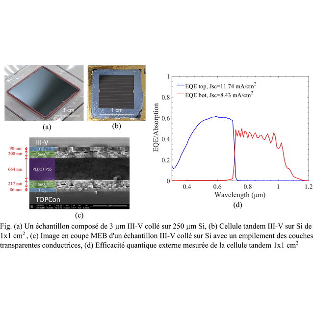
95% de la production photovoltaïque totale en 2020 est réalisée à partir de silicium. À l'échelle du laboratoire, le rendement record des cellules solaires silicium simple-jonction a atteint 27.6%, proche du rendement limite théorique de 29.4%. Une alternative pour mieux exploiter le spectre solaire consiste à combiner plusieurs semi-conducteurs dans des cellules solaires tandem, avec un rendement théorique de près de 45% pour une cellule solaire tandem optimale à double-jonction à base de Si. Les meilleures performances ont été obtenues par collage direct de III-V sur Si, mais la mise à l’échelle de cette technologie est difficile.
Dans cette thèse, nous avons conçu et développé une nouvelle méthode de collage, potentiellement peu coûteuse, pour les cellules solaires tandem III-V sur silicium à deux terminaux, basée sur des couches transparentes conductrices (TCL). Cet empilement de TCL est composé de deux revêtements antireflets (ARCs) dérivés de sol-gels et d'une couche à faible indice de réfraction. Les ARCs assurent des contacts ohmiques avec les sous-cellules et la transmission des photons de faible énergie à la cellule de silicium. La couche à faible indice de réfraction assure à la fois l'interconnexion électrique entre les sous-cellules et un meilleur recyclage des photons dans la cellule supérieure (gain d'efficacité pouvant atteindre 0.9% en valeur absolue). L’empilement TCL a été optimisé à l'aide d'outils de simulation optique afin d'obtenir une concordance de courant avec une perte de courant minimale, similaire au cas de l'architecture à collage direct. Le processus de laminage est réalisé dans l'air, à basse température de polymérisation (120°C) à l'aide d'une simple presse hydraulique. Un processus de photolithographie reproductible et robuste à une basse température de 80°C a également été optimisé avec succès. Nous avons fabriqué une première génération de cellule tandem AlGaAs/TCLs/Si ayant une surface de 1 cm2, avec une cellule Si de type TOPCon et une colle à base de PEDOT:PSS, qui montre des résultats prometteurs. Une stratégie de piégeage de la lumière utilisant une couche nanostructurée insérée à l'arrière de la cellule supérieure a également été explorée par des simulations électromagnétiques, en tenant compte des contraintes pratiques. Cette stratégie permet de minimiser l'utilisation de matériaux III-V par un facteur de 2.6.
Link: https://us02web.zoom.us/j/89732786691?pwd=MGNUbkNCS05vRUNhZEx2Z2dlTDJPUT09
Find a link in the the attached file below