
PhD defense

(in french)
C2N - Centre de Nanosciences et de Nanotechnologies, Amphithéâtre, PalaiseauPhD defense

(in french)
Télécom SudParis, Institut Polytechnique de Paris, , PalaiseauPhD defense

Hybrid silicon photonics based on magneto-optical materials
C2N - Centre de Nanosciences et de Nanotechnologies, Amphithéâtre, PalaiseauPhD defense
Jury members:
Mme Giovanna CALÒ - Rapportrice
M. Xavier LETARTRE - Rapporteur
M. Olivier GAUTHIER-LAFAYE - Examinateur
M. François ROYER - Examinateur
Mme Nathalie BARDOU – Examinatrice
Directeurs de thèse :
Mme Béatrice DAGENS
M. Laurent VIVIEN
Nonreciprocal optical devices, such as isolators and circulators, are essential for controlling light propagation in photonic systems. They prevent feedback-induced instabilities in lasers and enable signal routing for feedback-based processing. As photonic integrated circuits advance, the integration of nonreciprocal devices must keep pace. While magneto-optical isolators excel in compactness, insertion loss, isolation ratio, and spectral bandwidth, their performance in TE polarization remains limited.
Inspired by magnetobiplasmonic approaches, this work proposes a transverse magneto-optical Kerr effect (TMOKE) coupled-waveguide system. This architecture leverages modal beating and evanescent coupling in silicon waveguides, combined with the magneto-optical (MO) effect, to achieve nonreciprocal operation. Like conventional evanescent couplers, the TMOKE-coupled-waveguide system performs beam division and recombination. With proper tuning, it functions as a 3-dB beam splitter, with outputs that are either in-phase or out-of-phase depending on the propagation direction. Simulations on a silicon platform with a MO garnet demonstrate 30-dB isolation over a 35nm bandwidth and a compact 500µm footprint.
Self-pulsing synchronization and optomechanical spiking with integrated nanocavities for analog computing
C2N - Centre de Nanosciences et de Nanotechnologies, Amphithéâtre, PalaiseauPhD defense
This thesis explores two topics at the intersection of nanophotonics, nonlinear dynamics, and neuromorphic engineering using integrated photonic and optomechanical crystal cavities.
In the first part, we investigate the synchronization of two self-pulsing photonic crystal nanocavities. Starting from the design, fabrication, and full characterization of a single self-pulsing cavity, we then study both unidirectional and bidirectional synchronization regimes. Rich dynamical phenomena are revealed, including multi-frequency locking, phase slips, and asynchronous states, all backed by detailed experiments and simulations.
In the second part, we turn to the spiking (all-or-none) dynamics of an electro-optomechanical crystal cavity. By combining optical and electrical control of the mechanical resonance, we achieve the spiking behavior, the manipulation of the spiking threshold, temporal summation, and refractory period—key ingredients of biological neuron-like behavior. Experimental results are in good agreement with our theoretical and numerical predictions.

Mid-infrared SiGe photonics: electro-optical frequency-combs and supercontinuum generation
C2N - Centre de Nanosciences et de Nanotechnologies, Amphithéâtre,PhD defense
Jury Members
Loïc Bodiou (Université de Rennes)
Victor Torres-Company (Chalmers University of Technology)
Giuseppe Leo (Université Paris-Cité)
Goran Mashanovich (Southampton University)
The on-chip integration of mid-infrared spectroscopy systems provides a way to make them more accessible. In this context, silicon (Si) photonics is an attractive means to achieve this, thanks to the high throughput manufacturing capabilities it offers. To overcome the limitations of the materials used in standard Si photonics, due to the absorption of silica (SiO2) beyond 3.5 µm and Si beyond 7 µm wavelength, the germanium (Ge)-rich graded silicon-germanium (SiGe) platform platform represents a potential candidate. Not only does it extend the wavelength range accessible by Si photonics, but it also allows to keep the compatibility with high-volume CMOS manufacturing processes. The objective of this thesis work is to generate broadband light from existing mid-infrared light sources, necessary for the realization of such an integrated spectroscopic system.
Figure : Demonstration of a wideband mid-infrared source through supercontinuum generation, covering up to 2 octaves in the mid-infrared, while using low pump powers compared to the state of the art.

Strain engineering in freestanding ferroelectric membranes
C2N - Centre de Nanosciences et de Nanotechnologies, Amphithéâtre, PalaiseauPhD defense
Jury Members
Mme Céline LICHTENSTIGER UNIVERSITÉ DE GENÈVE, Rapporteure
M. Guillaume NATAF Université de Tours Rapporteur
M. Jean François DAYEN Université de Strasbourg Examinateur
M. Pavlo ZUBKO University College London Examinateur
M. Stéphane FUSIL Laboratoire Albert Fert - CNRS Invité
This thesis investigates the fabrication and controllable manipulation of freestanding ferroelectric oxide membranes, with a particular focus on strain and flexoelectricity as levers for tuning polarization. In contrast to conventional substrate-clamped thin films, released membranes possess enhanced mechanical freedom, providing a direct platform to probe how strain gradients influence ferroelectric behavior.
Using a sacrificial-layer release method, we fabricated freestanding membranes of archetypal ferroelectrics such as PbZrTiO₃ (PZT) and BaTiO₃ (BTO). We first explored their response under passive, uncontrolled bending conditions. These deformations induced polarization reorientation within the membranes, revealing bending as a functional route for engineering ferroelectric polarization.
To achieve deterministic control, we then developed an on-demand method to shape the membrane and prescribe strain with precision. This approach employs photoactive azobenzene polymers (PAZO), where UV illumination generates periodic surface relief patterns that mechanically deform the membrane. A spatial light modulator sculpts the illumination profile, and thus the strain field, with high fidelity. Through this light-written strain, we realize 90° polarization rotations in PZT via piezoelectric coupling and full 180° reversals in BTO driven by flexoelectricity, all in a periodic and programmable manner
Together, these results illuminate the intertwined roles of strain and flexoelectricity in ferroelectric materials and establish a versatile platform for probing and harnessing these effects with unprecedented control.
Figure : Photosensitive polymer platform for advanced ferroelectric strain engineering
(in french)
C2N - Centre de Nanosciences et de Nanotechnologies, Amphithéâtre, PalaiseauPhD defense

Coherent acoustic phonons in nanostructures: transduction, transport, and tunability
C2N - Centre de Nanosciences et de Nanotechnologies, , PalaiseauPhD defense
Coherent acoustic phonons are collective lattice vibrations with a well-defined phase. Their ability to couple with various excitations makes them attractive for interfacing different solid-state platforms, while their slow propagation speed enables signal processing and information storage in compact devices. In this thesis, we develop three nanophononic devices that address coherent phonon generation and detection, propagation control, and tunability. We introduce elliptical micropillar optophononic resonators that lift the degeneracy of optical cavity modes in energy and polarization. By combining this property with a cross-polarization-scheme pump-probe experiment, the generation and detection of coherent acoustic phonons are simultaneously enhanced. We design a phononic waveguide and demonstrate a quasi-continuous source of acoustic phonons at 20 GHz. We observe phonon propagation over 20 μm and demonstrate spatio-temporal coherent control of guided phonons. And finally, we design acoustic resonators incorporating mesoporous thin films and use their stimuli-responsive properties to achieve tunability of acoustic resonances through external environmental control. These three nanophononic devices serve as basic building blocks for phononic networks and advance the control of coherent acoustic phonons for classical and quantum applications.
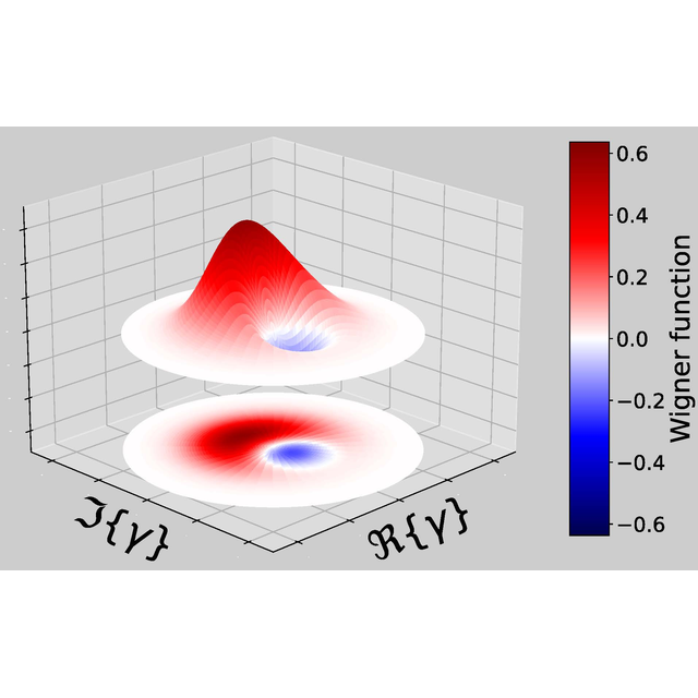
Wigner functions of Quantum Light emitted by Quantum Dot Sources
C2N - Centre de Nanosciences et de Nanotechnologies, Amphithéâtre,PhD defense
Semiconductor quantum dots have emerged as excellent single-photon sources for optical quantum technologies. When inserted in an optical cavity, they have been shown to deterministically emit pure, indistinguishable single photons on demand with high emission rates. Quantum dot single-photon sources have so far been used to process the quantum information that is encoded in the discrete modes of the single photons; a framework known as discrete-variable encoding. Alternatively, the quantum information can be encoded on the continuous quadratures of the optical field in the continuous-variable framework. With their ability to generate deterministically complex non-Gaussian states of light and to provide optical non-linearity at the single-photon level, quantum dots in cavities could also bring new opportunities to process the information in continuous-variable approach.
In this Ph.D. thesis, we take the first step toward positioning our quantum dot sources as potential resources for continuous-variable optical quantum technologies. We report on the first Wigner function measurement of the single-photon state and photon-number superposition states generated by an optical solid-state quantum emitter. We achieved this goal by overcoming key challenges in operating in the low-transmission regime and in adjusting measurement techniques to the high rate of our single-photon sources: (i) the optimization of the quantum interference between the local oscillator (a weak coherent state) and the photonic states emitted by our quantum dot device, which leads to optimal displacement operations, (ii) the correction of photon loss, and (iii) the reconstruction of photon-number distribution from single-photon detection.

Shaping tungsten dichalcogenides properties by chemical vapor deposition of alloys and polytypes
C2N - Centre de Nanosciences et de Nanotechnologies, , PalaiseauPhD defense
Two-dimensional (2D) transition metal dichalcogenides (TMDs) present varied optical and electronic properties associated with their different crystal structures. We optimize here the chemical vapor deposition (CVD) of tungsten-based TMDs, such as hexagonal (1H) WSe2 and WS2 monolayers, as well as monoclinic (1T’) WTe2. While 1H WSe2 and WS2 are typically direct band-gap semiconductors in the monolayer form, the anisotropic 1T' WTe2 is a small band gap topological insulator. Our purpose is to study the structural and electronic phase transition of ternary alloy WSe2xTe2(1-x) between the 1H and 1T' crystal structures. However, the synthesis of the mid-composition (x~0.5) alloys by CVD remains challenging. By just adding an additional monolayer, we obtain bilayer (2ML) structures, in which the available polytypes combinations, and the relative physical properties, are even richer. We further optimize our CVD growth methods to maximize the yield of 2ML hexagonal WSe2 and WS2. In addition to Raman and photoluminescence spectroscopies, we employ various other experimental techniques, including second harmonic generation and selective area electron diffraction, to discern between the 2ML polytypes. We then focus on the 3R bilayer stacking of WSe2 and we resolve its electronic band structure by angle-resolved photoemission spectroscopy.