







Direct orientation contrast imaging of zinc-blende III-V materials is studied using scanning electron microscopy. A quantitative approach is taken using a 3 µm thick orientation-patterned GaP grown on GaAs sample, studying the anti-phase domain contrast with respect to the electron beam energy and the tilt angle. A qualitative approach is taken for III-V grown on non-polar materials with and without chemical mechanical polishing. Finally, a processing of the acquired image for GaP on Si reveals in plane preferential anti-phase boundaries.
Currents methods for studying the inverted orientations of III-V semiconductors are either destructive, complex or time-consuming. A non-destructive, fast and direct imaging technique would be a key asset for the development of III-V based photonic and energy devices. In this work, leaded by a strong and historical collaboration between C2N and FOTON, with additional contribution of IHP, Thales Research & Technology and III-V Lab, we propose the use of a scanning electron microscope (SEM) equipped with an “in-lens” detector for the direct, non-destructive observation of anti-phase domains (APD) using the direct orientation contrast imaging (DOCI) technique.
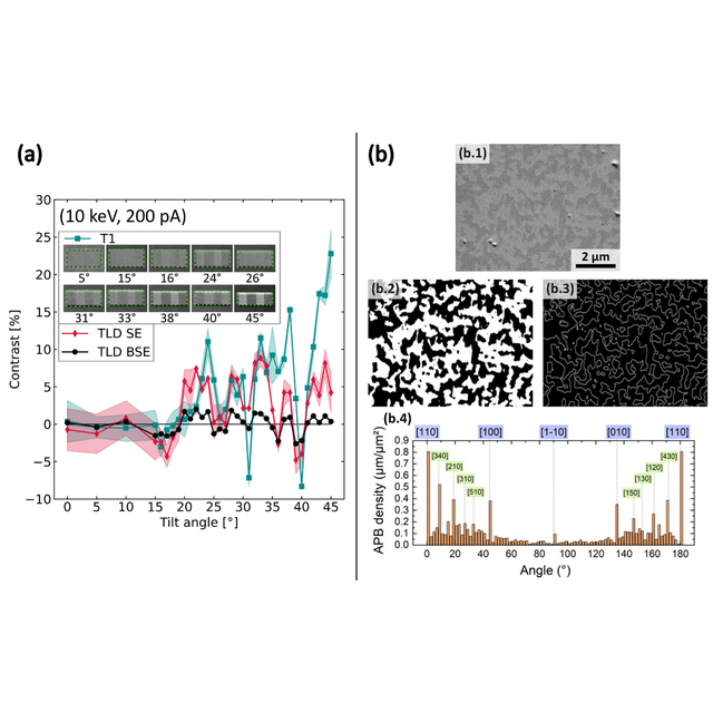
Two approaches are considered: a quantitative study on a reference sample where the distribution of antiphase domains is artificial and controlled (orientation-patterned gallium phosphide (OP-GaP) on GaAs), in which the effect of electron beam energy and sample tilt angle on the contrast of domains with inversed crystal orientations is measured using two different SEMs (a Thermo Fisher Scientific Verios G4 HP located at C2N, and a Thermo Fisher Scientific Apreo 2C located at FOTON); and a qualitative study of III-V samples epitaxially grown on nonpolar substrates, with and without chemically mechanical polishing, where the distribution of antiphase domains is natural.
The results confirm that this technique effectively detects the presence of antiphase domains under various experimental observation conditions. Furthermore, image processing performed on GaP grown on silicon reveals a preferential orientation of the antiphase walls in the growth plane. This makes the technique ideally suited for both very thin films and thick samples, as well as for a wide variety of electron microscopes. It also makes DOCI a relevant technique for statistical analyses of APDs and APBs. DOCI should therefore serve as a relevant method for imaging and characterizing APDs on other non-centrosymmetric materials and could be useful, for instance, in controlling of the quasi-phase matching period in orientation-patterned materials or in epitaxy studies on APDs annihilation.
References :
Direct orientation contrast imaging of antiphase domains on III-V materials using scanning electron microscopy
Brieg Le Corre1,2, Clothilde Grenèche2, Rozenn Bernard2, Tony Rohel2, Antoine Létoublon2, Wijden Khelifi2, Julie Le Pouliquen2, Arnaud Grisard3, Sylvain Combrié3, Bruno Gérard4, Abdelmounaim Harouri1, Luc Le Gratiet1, Grégoire Beaudoin1, Konstantinos Pantzas1, Isabelle Sagnes1, Oliver Skibitzki5, Gilles Patriarche1, Charles Cornet2 and Yoan Léger2
Phys. Rev. Materials 10, 073804
DOI: https://doi.org/10.1103/vl71-8m3d
Affiliations
1Centre de Nanosciences et de Nanotechnologies, CNRS, 91120 Palaiseau, France
2Univ Rennes, INSA Rennes, CNRS, Institut FOTON, UMR 6082, F-35000 Rennes, France
3Thales Research and Technology, 91767 Palaiseau, France
4III-V Lab, 91767 Palaiseau, France
5IHP-Leibniz Institut für Innovative Mikroelektronik, 15236 Frankfurt (Oder), Germany
Figure : (a) Orientation contrast evolution on OP-GaP, with their 70%-confidence interval, with respect to the tilt angle for beam energy of 10 keV using T1, TLD-SE mode and TLD-BSE mode represented in dark cyan, crimson and black respectively. Insets are post-processed SEM images of T1 measurements done OP-GaP (region of interest within the green rectangle, containing four domains which have alternating crystallographic orientation). (b) Statistical analysis done on a GaP on Si sample: (b.1) DOCI of the two opposite APDs with tilt correction. (b.2) Multistep thresholding binarization of (b.1). (b.3) Edge detection of (b.1) highlighting the existing APBs. (b.4) Determination of APBs densities with respect to angle after Hough transform done on (b.3).
Contact : Brieg Le Corre
Acknowledgments – This work was supported by the French RENATECH network, by "France 2030" with the French National Research agency OFCOC project, by the French National Research agency PIANIST project, NUAGES project and NANOFUTUR project, and by the EUROPEAN Union (101088331 – PANDORA). This research was also supported by the European Union through European Regional Development Fund (ERDF), Ministry of Higher Education and Research, Brittany region, Conseil Départemental d’Ille-et-Vilaine, Rennes Métropole, through the CPER Project PhotBreizh.