A unique instrument has been developed to grow nanocrystals by molecular beam epitaxy in a transmission electron microscope. The crystal formation is observed in situ and in real time with the atomic resolution.
Nanotechnology uses nano-sized crystalline materials that can be fabricated by different techniques. Understanding and controlling the formation of these nanocrystals represents a major challenge to master their properties and thus achieve a given functionality. To probe and to study their morphology, crystalline structure or chemical composition, transmission electron microscopy (TEM) is a technique of choice. Indeed, the TEM analyzes can be conducted at the atomic scale. In the recent years, an impressive improvement of their spatial resolution has been achieved, enabled by the development of aberration correctors.
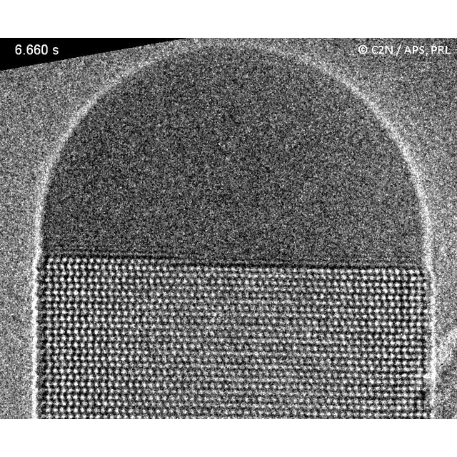
Molecular beam epitaxy (MBE) is known as an ultimately precise technique for growing thin films or nanostructures of semiconductors or metals. This technique has never been implemented before in an operational transmission electron microscope. This instrumental challenge has been recently achieved within the framework of the NanoMAX project, by researchers and engineers from the Centre de Nanosciences et de Nanotechnologies (C2N, CNRS / Univ Paris-Sud) and the Laboratoire de physique des interfaces et des couches minces (LPICM, CNRS / École Polytechnique). They have observed in real time and at the atomic scale the formation of gallium arsenide (GaAs) nanowires. These nanowires grow from atomic or molecular beams of gallium and arsenic directed to a thin heating membrane, transparent to the electron beam of the microscope. The membrane is covered with gold nanoparticles that catalyze the growth of nanocrystals. With this preparation, the atomic layers of the crystal grow one by one at the interface between the nanowire and the catalyst droplet.
Each new atomic layer begins with a convex boundary. Indeed, this configuration minimizes the total length of this boundary. Then, during the layer spreading, the curvature of the boundary is reversed: the edge of the layer prefers to elongate at the periphery of the droplet than inside the liquid. This configuration remains until the layer is completed. The researchers interpreted these observations using a simple model based on the geometry of the system. They consider a lower energy per unit length of the layer boundary at the periphery than inside the liquid droplet. This characteristic layer progression thus allows the system to minimize its energy.
More generally, the use of this original NanoMAX equipment opens access to crucial information on the mechanisms involved during the growth of nanostructures. This includes the morphology of the catalyst, the structure of the growth front, the location of layer nucleation or the kinetics of the atomic step flow. This knowledge will lead to a better control of the nanocrystal properties. Finally, other sources of matter can be fitted to this unique instrument and a wide range of materials - semiconductors, carbon objects, metals, oxides – can be studied. A great tool for material sciences!
References:
Atomic step flow on a nanofacet
J.-C. Harmand, G. Patriarche, F. Glas, F. Panciera, I. Florea, J.-L. Maurice, L. Travers and Y. Ollivier
Physical Review Letters, 121, 166101 (2018)
DOI : 10.1103/PhysRevLett.121.166101
- Centre de nanosciences et de nanotechnologies (C2N, CNRS/Univ. Paris-Sud)
- Laboratoire de physique des interfaces et des couches minces (LPICM, CNRS/École Polytechnique)
- The publication was featured on the Physics website of the American Physical Society (APS) : Focus : Video—Growing a Crystal One Atomic Layer at a Time
Contact
Jean-Christophe Harmand, CNRS Senior Researcher at C2N
Figure: Growth of the GaAs wurtzite structure in a tilted view revealing a two-dimensional projection of the atomic step flow. Each successive atomic layer starts at the triple phase line, boundary between the solid, liquid and vapor phases. When the monolayer covers about 75% of the solid / liquid interface, an inversion of the step curvature in the liquid is observed. This phenomenon reveals that the effective energy per unit length of monolayer edge is much lower at the interface periphery than inside the catalyst droplet. © C2N, CNRS / Université Paris-Sud