
PhD defense
Integrated nonlinear optics with hybrid integration of 2D materials
C2N - Centre de Nanosciences et de Nanotechnologies, , PalaiseauPhD defense
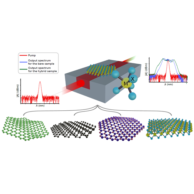
La photonique intégrée offre des réponses aux limitations de la microélectronique mais certains effets tel que les effets d'optique nonlinéaires sont difficile à générer. En intégrant des matériaux 2D aux propriétés non linéaires exceptionnelles, ces limitations peuvent être surmontées. Les outils numériques sont utilisés pour la conception et l'optimisation des guides d'ondes, en tenant compte de l'impact des matériaux 2D sur les paramètres sensibles de la structure photonique. De premiers essais s'appuyant sur l'exfoliation mécanique permet de fabriquer et transférer des matériaux 2D sur les guides d'ondes. Au regard des résultats, et malgré une première demonstration des développements supplémentaires sont nécessaires pour surmonter les limitations liées à la taille des feuillets de matériau, aux dépôts involontaires et à la faible répétabilité des transferts.
Différentes strategies sont ainsi mises en place pour l'optimisation des structure hybrid. Cela s'effectue en trois axes distincts. Tout d'abord, l'optimisation des paramètres optogéometriques des tructures guidantes permet l'augmentation de l'interaction entre les matériaux bidimensionnels et le mode transverse améliorent les performances non linéaires des guides. Ensuite, les méthodes de transfert peuvent être améliorié afin d'augmenter la fiabilité des transfert ainsi que la surface couverte par les matériaux 2D. Le dévelopment de méthodes permettant le transfert ciblé de matériaux fabriqués par CVD offrent des surfaces de meilleure qualité et une plus grande homogénéité, facilitant le transfert de larges surfaces de matériaux. Des résultats prometteur de dépôt en large surface (2.8mm x 3.2 mm) de matériaux 2D ont été obtenus.
Enfin, l'utilisation de cavités en anneau permet une amélioration notable de l'interaction entre les matériaux 2D et l'onde en exploitant les effets de résonance. Des études expérimentales de résonateurs en anneau hybrides ont été réalisées, démontrant le potentiel de cette approche.
Ces avancées ouvrent de nouvelles perspectives dans la photonique intégrée, améliorant les performances non linéaires des guides hybrides et ouvrant la voie à de nouvelles applications dans les communications optiques, le traitement optique de l'information et d'autres technologies photoniques avancées.
Coupling of thermoelectric and electrochemical measurements in microfluidics for microRNA detection
C2N - Centre de Nanosciences et de Nanotechnologies, , PalaiseauPhD defense
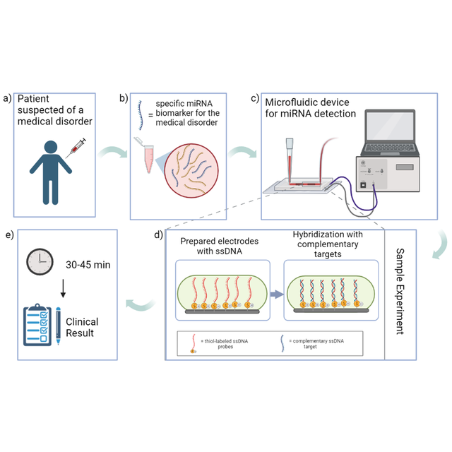
Circulating microRNAs (miRNAs) are short non-coding RNAs composed of 19-25 nucleotides and present in various bodily fluids, including blood, serum, saliva,urine, and breast milk. The alteration of miRNA expression has been deeply investigated in recent years, and it was found to be associated with several disorders comprising cardiovascular diseases, cancers, and neurodegenerative conditions. In this context, Dr. Gamby at the Center for Nanoscience and Nanotechnology (C2N) launched some research projects to develop microfluidic platforms for miRNA detection via electrochemical biosensors. My Ph.D. thesis aims to design, fabricate and characterize a microfluidic device that can detect mi-croRNA (miRNA) by coupling thermoelectric and electro-chemical measurements.
Electrochemical biosensors are transducers in contact with the analytes under detection, transforming physical or biochemical reactions into an electrochemical signal. The biosensor utilizes single-stranded DNA (ssDNA) probes immobilized on the electrode surface to recognize the target miRNA molecules. Moreover, integrating the thermal sensor permits measuring the heat released during the hybridization between the ssDNA probe and the miRNA target, which is peculiar to each sequence, allowing higher specificity to the detector. In this Ph.D. thesis, I present two microfluidic devices englobing different sensors. Notably, the electrochemical biosensor employs gold for the first device and platinum for the second one. In addition, the first chip is equipped with a thermopile, while the second one comprises a resistance thermal detector (RTD). The second microfluidic device developed permitted the electrochemical detection of the target miRNAs at three concentrations: 10−14 M, 10−10 M, and 10−6 M. Moreover, real sample experiments are conducted, allowing distinguishable results between wildtype mice milk presenting normal levels of miRNA 30b and transgenic milk samples enriched with miRNA 30b. In parallel, the microcalorimeter permitted real-time monitoring of the self-assembled monolayer formation with ss-DNA probes.
The schematic explains the aim of microfluidic devices for miRNA detection: a) A bodily fluid test analysis is performed to a patient. b) The test aims to quantify a specific miRNA that has been identified as biomarker for a medical disorder. c) The analysis can be conducted in a simple laboratory by the use of the microfluidic chip. d)The biosensors permit the detection and quantification of the target miRNA by biorecognition. e) Providing faster results compared to traditional methods.
Novel optical devices with non-Hermitian physics
C2N - Centre de Nanosciences et de Nanotechnologies, , PalaiseauPhD defense
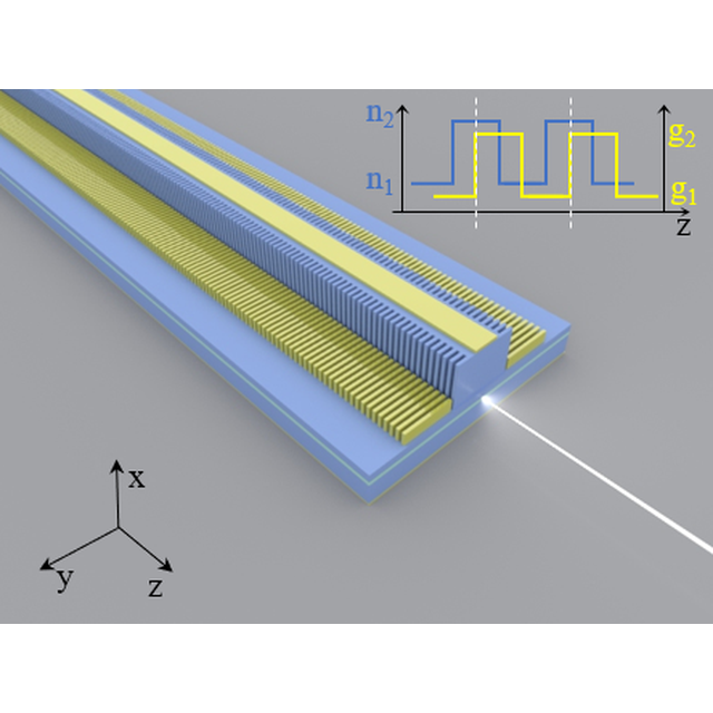
This PhD thesis deals with the development of a new concepts of optical sources exploiting the concept of Hon-Hermitian physics. To this end, two new approaches in the non-Hermitian formalism for achieving single-frequency lasers have been proposed and demonstrated. One demonstration is applying the concept of PT symmetry to the platform of first-order complex coupled Bragg grating distributed feedback lasers. Lower threshold and higher output power, as well as more stable single-frequency emission, were achieved compared to previous work with a PT-symmetric grating operating at third order. An asymmetrical behavior of the external feedback resistance with respect to the phase arrangement modulation for the real and imaginary parts of the PT-symmetrical grating was observed. A complementary concept, still based on the non-Hermitian formalism, exploiting gain-loss modulation using metamaterial gratings to realize single-frequency lasing was experimentally demonstrated at a working wavelength of 1.55 µm. A robust single-frequency laser emission, with an SMSR of 70 dB, was obtained. The concept of non-Hermitian physics has also been applied to the study of optimal detection using Fano resonant metasurfaces. The control of Fano resonance asymmetry and sharpness obtained by navigating between dark mode conditions and exceptional points was demonstrated. Optimal operations with single-layer and double-layer metasurfaces were discussed. The introduction of the third dimension into the system allows greater flexibility to manipulate the spectral response. New additional features resulting in cliff-like Fano resonance have been obtained in the case of an identical double-layer metasurface with deep sub-wavelength cavity length. In addition, tunability mechanisms based on the variation of gain or loss in such types of system have been discussed. The conditions required to reach the dark mode condition corresponding to the lasing threshold have been established.
Figure :
Strain modulation of magnetic domain wall motion in CoFeB systems
C2N - Centre de Nanosciences et de Nanotechnologies, , PalaiseauPhD defense
Strain-induced modification of magnetic properties in hybrid piezoelectric/ferromagnetic heterostructures is being intensively investigated due to its potential for low-power spintronics applications based on magnetic domain wall (DW) motion. Materials with in-plane magnetic anisotropy (IPA) and perpendicular magnetic anisotropy (PMA) have been used to study strain-induced magnetization variations in hybrid piezoelectric/ferromagnetic heterostructures. However, from a fundamental perspective, a comprehensive understanding of the magnetic DW velocity dependence on various strain configurations (such as uniaxial, biaxial, and shear strains) and geometries is still lacking, particularly in PMA materials. Therefore, more fundamental research is needed to understand the role of electric field-tuned piezoelectric and ferromagnetic coupling and its impact on magnetic DW motion for the development of energy-efficient strain-induced devices. This thesis aims to investigate the effect of different strain configurations and geometries on magnetic DW motion in PMA materials. This work investigated the influence of piezoelectric strain on magnetic DW motion in PMN-PT (011)/Ta/CoFeB/MgO-based devices through two distinct approaches. The first approach studied the effect of biaxial in-plane strain and out-of-the-plane polarization on DW motion in continuous magnetic films on top of piezoelectric substrates. In contrast, the second approach explored the impact of local uniaxial in-plane strain on DW velocity modulation in patterned devices. The first results presented in this thesis show that, in PMN-PT (011), the application of a voltage along the sample's out-of-plane (OOP) direction leads to a non-volatile polarization state, as confirmed by piezoresponse force microscopy. In this configuration, we observe a non-volatile decrease in the DW velocity during the creep regime in the poled state with respect to the unpoled state. This response can be linked not only to a strain-control of magnetic anisotropy but also to a strain-controlled change in the homogeneity of the magnetic landscape. Such interface modulations result in additional pinning sites in the poled state compared to the poled state, as confirmed by our creep dynamics analysis. This can significantly affect DW nucleation/depinning fields, which opens the door to using strain to control magnetic disorder. The second result of this thesis explores the effect of annealing on hybrid piezoelectric/ferromagnetic heterostructures, revealing significant impacts on DW velocity and anisotropy modulation. Despite the strain relaxation in the PMN-PT layer, our measurements showed a significant reduction in the DW velocity in the creep regime after annealing. This reduction in velocity was attributed to the increased effective anisotropy in the annealed state, which resulted from the improvement of the crystalline structures of CoFeB and MgO induced by the high annealing temperature. Our FMR measurements confirmed that this partial crystallization enhanced the PMA compared to the as-grown state. Therefore, our results showed that recovering the magnetic DW velocity to its original as-grown state was impossible after annealing. Additionally, a DW velocity modulation of up to 50% in the presence of local in-plane strain was observed, which was attributed to anisotropy modulation at the local scale. Finally, in the last part of the thesis, micromagnetic simulations were performed to validate and interpret our observed experimental results on strain-influenced DW dynamics modulation beyond the creep regime in continuous magnetic films on top of piezoelectric substrates. In summary, this study offers significant contributions toward understanding the behavior of magnetic DWs in response to different strain configurations. Multiple strain configurations in piezoelectric/ferromagnetic hybrid structures can open new opportunities for the electrical manipulation of DW dynamics.
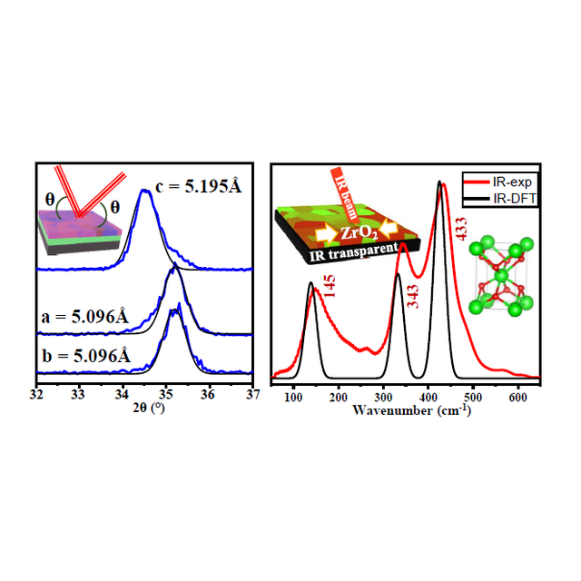
Crystal Phases and Electro-Optic Properties of ZrO₂ and HfO₂ Ferroelectric Thin Films
C2N - Centre de Nanosciences et de Nanotechnologies, , PalaiseauPhD defense
The ferroelectricity in ZrO₂ and HfO₂ oxides was discovered in 2011 in ultrathin layers and has garnered significant attention for its potential applications in microelectronics. These materials offer the advantage of maintaining ferroelectric properties even at thicknesses below 10 nm, which is considerably thinner than perovskite ferroelectrics. Additionally, they are compatible with silicon and can be readily integrated into silicon foundries. As non-centrosymmetric crystals, ZrO₂ and HfO₂ ferroelectrics are expected to exhibit an even nonlinear response, characterized by nonlinear susceptibility terms such as χ⁽²⁾. Based on this effect, these materials can also be explored for electro-optic applications in silicon photonics. However, the low thickness that is advantageous for microelectronic applications becomes a drawback for photonic ones. Therefore, the initial challenge is to increase the thickness of ZrO₂/HfO₂ ferroelectric thin films to approximately 50 nm to make them suitable for photonic devices. Our research demonstrates that pure ZrO₂ can maintain a ferroelectric state at a higher thickness compared to HfO₂, reaching approximately 40 nm (versus 10 nm in HfO₂). Moreover, through first-principle calculations, we demonstrate that ZrO₂ exhibits higher electro-optic (EO) coefficients compared to HfO₂, making ZrO₂-based ferroelectrics an attractive candidate for further research to optimize them for electro-optic applications.
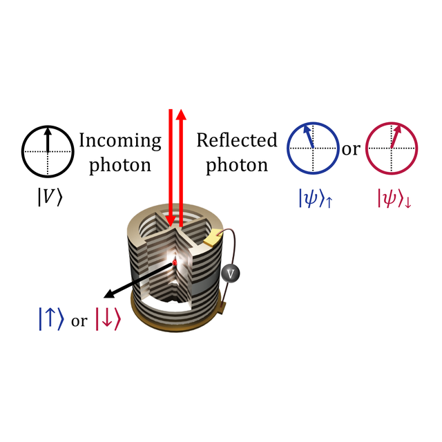
Giant polarisation rotation with a quantum dot-based spin-photon interface
C2N - Centre de Nanosciences et de Nanotechnologies, , PalaiseauPhD defense
The development of an interface between stationary qubits and messenger qubits offers many possibilities for quantum communications, via the exchange of information between qubits, and for quantum computation, via the realisation of logic gates and/or complex, multi-entangled quantum states. In this context, we study a semiconductor quantum dot system embedded in a micropillar optical cavity. Such a system allows the trapping of an electron whose spin can interact with an incident photon: the polarisation of the reflected photon is then modified according to the spin state of the electron. The objective of such an interface is to obtain a perfect mapping between the spin state and the polarisation state of the photon after interaction with the quantum dot. This results in a giant polarisation rotation of the photons reflected by the studied system, the direction of which is spin-dependent. We have therefore developed an expertise in the generation of specific polarisation states, as well as in the measurement of arbitrary polarisation states, in order to analyse the polarisation response of the quantum dot-micropillar device. We then demonstrate the possibility of reaching a giant polarisation rotation that depends on the spin state of the electron. The measurement of this rotation is enabled by a full polarisation tomography. Finally, we study the efficiency of the spin state projection induced by the detection of a photon reflected by the system, in order to characterise the performance of our spin-photon interface. This work opens up possibilities towards the realisation of efficient spin-photon interfaces, based on charged quantum dot-cavity devices.
Figure : Scheme of an electrically contacted pillar microcavity coupled to a charged quantum dot. The polarisation of reflected photons is rotated through the interaction with the embedded spin qubit.
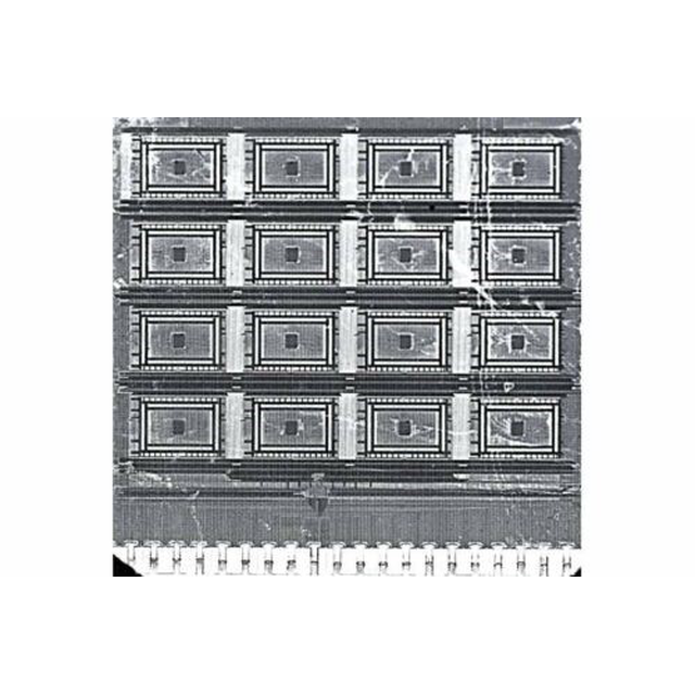
Energy-Efficient Memristor-Based Artificial Intelligence Accelerators using In/Near Memory Computing
C2N - Centre de Nanosciences et de Nanotechnologies, , PalaiseauPhD defense
Artificial Intelligence (AI) is increasingly impacting our daily lives, promising transformative changes across numerous societal domains. However, AI faces two major hurdles : energy efficiency and trustworthiness. High energy demands of AI contribute to global carbon emissions and limit its usage in resource-limited environments. Meanwhile, AI's 'black box' nature raises concerns about its reliability, hindering wider acceptance. This thesis addresses these challenges by bringing together AI, computer architecture, and emerging technologies. Our key strategy is the development of specialized integrated circuits utilizing cutting-edge memristor technology, a nanoelectronic technology designed to support low-energy computational paradigms for AI models, specifically in resource-constrained contexts. We exploit memristors' non-volatility and in/near-memory capabilities for higher energy efficiency, especially in edge computing. Additionally, we incorporate Bayesian inference, an explainable AI technique, to enhance the transparency and trustworthiness of AI.
Figure : An optical microscopy image of our Memristor-Based Bayesian machine

(in french)
C2N - Centre de Nanosciences et de Nanotechnologies, , PalaiseauPhD defense

(in french)
C2N - Centre de Nanosciences et de Nanotechnologies, ,PhD defense
Les cellules solaires en couche mince, constituées de semiconducteurs à bande interdite directe d'une épaisseur de 2 à 4 μm, constituent une alternative attractive aux cellules conventionnelles formées de 150 μm de silicium. Elles permettent une faible consommation de matériaux et une empreinte carbone réduite. Avec une réduction supplémentaire de l’épaisseur d’un facteur 10, les cellules solaires ultrafines offrent de nouvelles possibilités pour économiser des matériaux rares, réduire le temps et le coût de fabrication, faciliter la collecte des porteurs de charge dans les absorbeurs, et étendre le champ des applications du photovoltaïque à des dispositifs flexibles ou tolérants aux rayonnements. Cependant, des stratégies de piégeage optique sont nécessaires pour compenser la faible absorption des films ultrafins, et elles doivent respecter des contraintes de conception et de fabrication exigeantes.
Cette thèse se concentre sur le développement de cellules solaires ultrafines en GaAs, un semiconducteur monocristallin de haute qualité qui a permis le record d'efficacité des cellules solaires à simple jonction, et en CdTe, un matériau polycristallin peu coûteux et adapté à la fabrication industrielle à grande échelle.
Dans une première partie, les pertes des cellules solaires précédentes en GaAs de 200 nm d'épaisseur sont analysées, et un nouveau design de piégeage optique est proposé. Il est constitué d’une couche nanostructurée à fort indice, qui est encapsulée dans un matériau mésoporeux à faible indice, avec un miroir plan en argent en face arrière.
Cette structure permet d'obtenir un courant de court-circuit théorique de 28,2 mA/cm². Une preuve de concept de cette cellule solaire ultrafine est démontrée, avec une réponse optique multi-résonante en accord avec les simulations numériques.
Afin d'améliorer encore l'efficacité globale des cellules solaires ultrafines, un nouvel empilement de couches basé sur une hétérostructure n-GaAs/p-AlGaAs de 250 nm d'épaisseur est introduit, le courant de court-circuit théorique atteint 28,9 mA/cm².
Une seconde partie est consacrée aux différents facteurs entravant le développement de cellules solaires CdSeTe/CdTe polycristallines ultrafines.
La passivation des défauts par l'incorporation de sélénium est étudiée par cartographie de cathodoluminescence à haute résolution. La diffusion des atomes de sélénium et leur impact sur l'efficacité radiative des alliages CdSeTe sont analysés quantitativement. Ensuite, plusieurs solutions pour un contact arrière ohmique, passivant et réfléchissant sur le CdTe sont explorées. Enfin, la stratégie de piégeage optique multi-résonante développée pour le GaAs ultrafin est adaptée aux contraintes technologiques des dispositifs en CdTe. Par simulation optique, une efficacité de conversion allant jusqu'à 19,5% est prédite dans une cellule solaire en CdSeTe de 200 nm d'épaisseur avec un contact arrière nanostructuré.
(in french)
C2N - Centre de Nanosciences et de Nanotechnologies, , PalaiseauPhD defense