
PhD defense
(in french)
C2N - Centre de Nanosciences et de Nanotechnologies, ,PhD defense

(in french)
C2N - Centre de Nanosciences et de Nanotechnologies, , PalaiseauPhD defense

Monolithic Isolate Interface for Bidirectional MOSFET Switches dedicated to the Control of Tuning and Energy Conversion Systems Used in Medical Applications directed
C2N - Centre de Nanosciences et de Nanotechnologies, , PalaiseauPhD defense

III-V-on-Si nanowire-based solar cells for tandem applications
Institut Photovoltaïque d'Île-de-France (IPVF), , PalaiseauPhD defense
Tandem PV technologies combining a III-V semiconductor cell over a silicon (Si) cell offer a promising pathway to exceed the efficiency limit of single junction Si solar cells (29.4%). Owing to their small diameters, nanowires (NWs) allow to mitigate the lattice constant and thermal coefficient mismatch issues associated with the direct growth of high-quality III-V layers on Si. The goal of this PhD work is to fabricate a high-efficiency solar cell consisting of first GaAs NWs, and ultimately GaAsP NWs, directly grown on Si by molecular beam epitaxy. First, the patterned Si substrate preparation process was optimized to obtain ordered GaAs NW arrays with near-perfect and reproducible vertical yields. Our champion core–shell GaAs/GaInP NW solar cell demonstrated a high Voc of 0.65 V, and an efficiency of almost 3.7%, at the state-of-the-art of radial junction GaAs NW solar cells grown on Si.
The calibrated photoluminescence characterization of these NW arrays indicated good optoelectronic properties, with a quasi-Fermi level splitting of 0.84 eV at 1 sun, and we identified significant room for device improvement. Increasing the n-type doping level in the NW shell could be one way of enhancing device performance. To this end, we used cathodo-luminescence to study the incorporation efficiency and homogeneity of tellurium in self-catalyzed GaAs NWs. Finally, GaAs/GaAsP/GaP axial junction NW solar cells were fabricated for the first time in our group. Luminescence characterization indicated pro- mising optoelectronic properties. Using electronic simulation, we attributed the limited performances to energy barriers at the n-type contact. Overall, this PhD work contributed to significant technological
advances, and the detailed characterization experiments and simulation results presented shed light on the potential and challenges of III-V-on-Si NW-based solar cells.
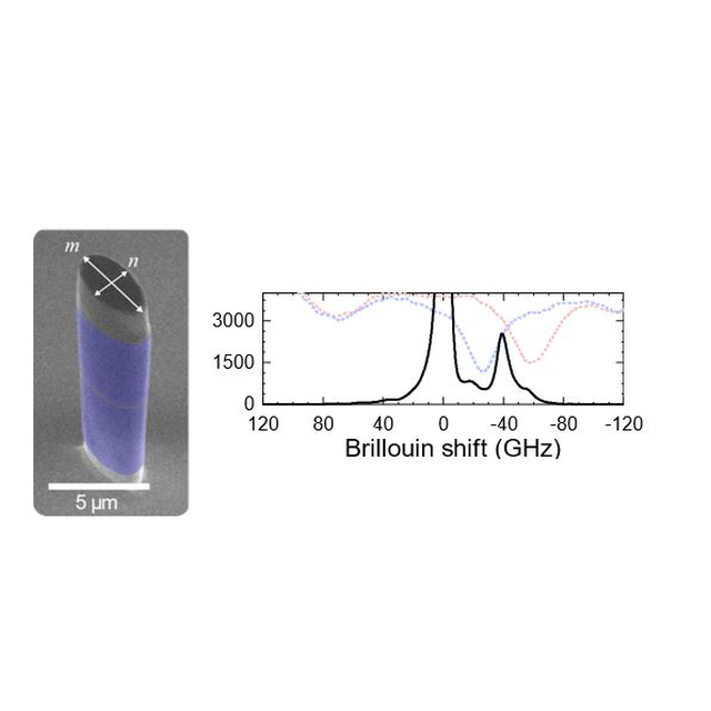
Brillouin scattering in optophononic heterostructures working at ultrahigh acoustic frequencies
C2N - Centre de Nanosciences et de Nanotechnologies, , PalaiseauPhD defense
Nanophononics, i.e. acoustic phonon engineering, is a promising research domain with potential in the manipulation of sound and heat at the nanometric scales. Research on the vibrational properties of systems formed by semiconductor multilayers has permitted to achieve a new level of understanding of acoustic phonons in these structures.
In this work, we introduce topological phononic devices made of semiconductor superlattices to control the propagation and confinement of acoustic phonons in the tens to hundreds of gigahertz range.
We developed Brillouin spectroscopy experimental schemes to access the confined acoustic modes in planar and micropillar optophononic cavities where both light in the near infrared range and acoustic phonons in the 20 GHz range can be simultaneously confined.
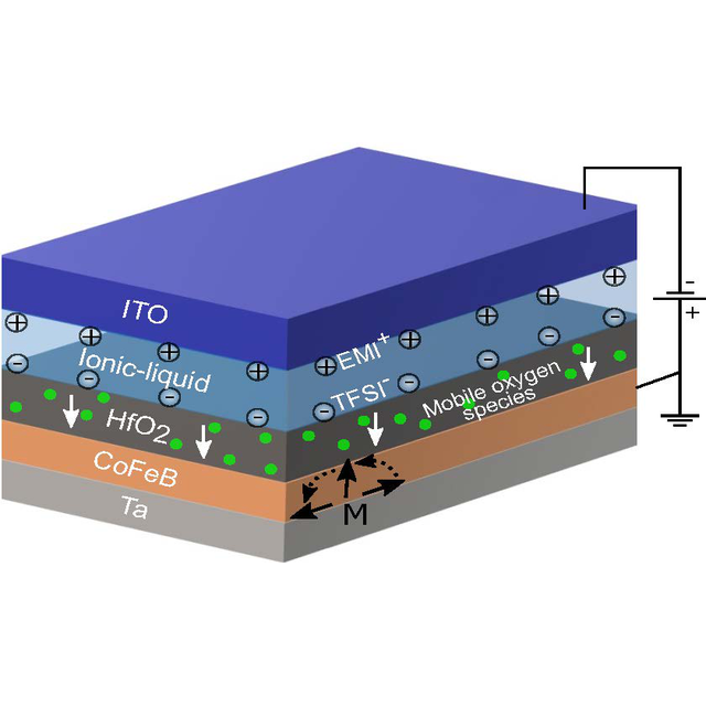
Magneto-ionics in CoFeB systems
C2N - Centre de Nanosciences et de Nanotechnologies, , PalaiseauPhD defense
Electric field control of magnetic properties in ferromagnetic thin films is a sought-after feature for spintronics devices, as it offers great potential for high energy efficiency in memory applications.
Much like the power efficiency, two other sought-after features to incorporate are nonvolatility and reversibility. In addition to the effects arising from electric field-induced charge accumulation at the ferromagnet/dielectric interface, electric field-induced migration of ions in dielectric layers adjacent to a magnetic layer shows a more extended effect, resolving electrostatic screening and volatility of charges. Such a technique is known as magneto-ionics. Magneto-ionic control of magnetic properties using oxygen ions has been of great importance in developing energy efficient spintronics devices; however, the magneto-ionic performance such as speed, reversibility and stability is largely influenced by the stack materials. In this thesis, CoFeB-based systems are explored for various heavy metal buffer layers optimizing magneto-ionic performance addressing the importance of factors such as the level of oxidation, post-growth annealing and the stability.
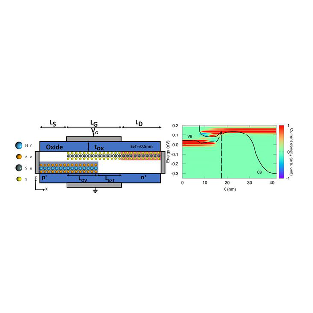
Semi-empirical and ab-initio simulation of quantum transport in nanoscale devices
C2N - Centre de Nanosciences et de Nanotechnologies, , PalaiseauPhD defense
The aggressive shrinking of transistor sizes by the microelectronics industry has reached the nanoscale. The performance of components at this scale is strongly impacted by quantum phenomena (tunnelling, interference, etc.) but also the electrostatic control becomes more delicate. In order to improve the performance of components, it is essential to take these phenomena into account and to explore alternatives to the silicon-based MOSFET that is the current reference. This task can be supported by a rigorous theoretical approach for electronic material properties and thus simulate the performance of the devices.
In this thesis, we propose to extend the state of the art in this field by developing an electronic transport model based on the non-equilibrium Green’s function formal-ism. The particularity of our approach is the use of pseudopotential Hamiltonians based on plane waves obtained by either a semi-empirical or an ab-initio approach. This type of Hamiltonian allows us to obtain an atomistic description of the material and thus to have an accurate description at the microscopic scale.
In a first part, we developed the empirical pseudopotential Hamiltonian model to study III/V material heterostructures (InAs/GaSb) with a non-abrupt inter-face. This method has been applied to the study of tunnelling based devices, Esaki diode and tunnel FET. The results show a degradation of the current when the transition region is long. A comparison with an experimental study also showed the accuracy of our simulations.
In the following parts of the thesis, the focus is on the Hamiltonians obtained from ab-initio calculations. We started with the development of a model to study the Hamiltonians of heterostructure by investigating two approaches, one based on the Hamiltonian of isolated material and the second based on the Hamiltonian of a supercell of the heterostructure. The models were applied to two components, a MOSFET composed of monolayer and bilayer PtSe2 and a tunnel FET composed of monolayer PdSe2 and monolayer SnS2. This highlighted that the study of the interface between two distinct materials requires the use of sophisticated approaches to describe the coupling between the materials. To improve the model, we then included electron-phonon interactions in our simulations. We first used deformation potentials, fully derived from ab-initio calculations, to describe the coupling with phonons under the self-consistent Born approximation. This model has been applied to the study of a tunnel FET made with the heterostructure of a monolayer HfSe2 and a monolayer SnS2. Two different architectures were studied, one with a vertical stacking of the 2D materials and a lateral heterostructure. The results show that phonons play an important role for the transmission properties by introducing an increase in current through inter-valley transmission. Finally, the vertical heterostructure emerges as the most promising candidate with a sub-threshold slope of 40 mV/dec for an ON state current of 580 mA/μm at VDD= 0.35 V.
In the last part of the thesis, a more rigorous description of the electron-phonon coupling for transport was proposed. We have developed a model using ab-initio calculations of the electron-phonon matrix elements and phonon frequencies. This model was compared to the literature and to the deformation potential method by studying the monolayer MoS2 with mobility calculations. Finally, the study of a CMOS was carried out using an n-type (with monolayer MoS2) and a p-type (with monolayer WSe2) MOSFET. Despite the phonon scattering, the devices satisfy the predictions for the next generation of transistors.
(in french)
C2N - Centre de Nanosciences et de Nanotechnologies, , PalaiseauPhD defense
(in french)
Centre de Nanosciences et de Nanotechnologies, Amphithéâtre,PhD defense